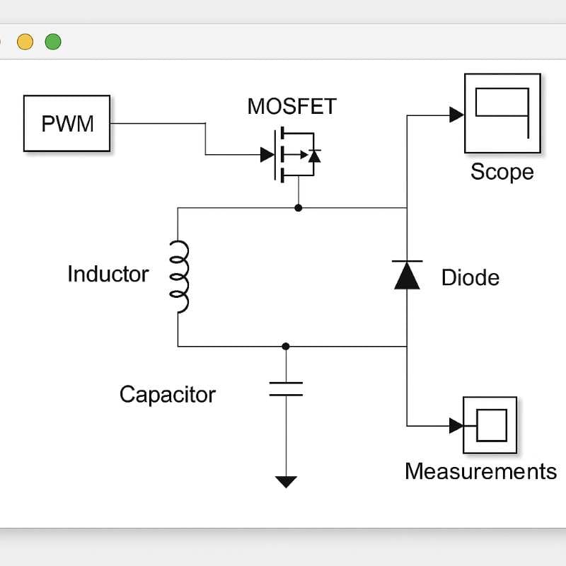
What is a Buck and Boost Converter?
A Buck and Boost Converter is a DC-DC circuit that steps down or steps up input voltage to provide a regulated, efficient, and stable output.
Thank you for reading this post, don't forget to subscribe!What is a Buck Converter?
A Buck Converter is a switching regulator that converts a higher DC voltage into a lower DC voltage. It conserves energy by transferring it through inductive storage instead of resistive dissipation.
What is a Boost Converter?
A Boost Converter is a DC–DC Step-Up converter that converts a low input voltage into a higher output voltage. It’s widely used in battery-powered systems, LED drivers, and renewable energy circuits.
1. Buck and Boost Converter Circuit
A Buck and Boost Converter Circuit is an advanced DC–DC switching regulator system that either steps down (Buck Converter) or steps up (Boost Converter) the input voltage.
It is one of the most essential circuits in power electronics, widely used in battery chargers, LED drivers, power supplies, and renewable energy systems.
In a Buck Converter, the output voltage is lower than the input, while in a Boost Converter, the output voltage is higher than the input.
⚙️ Basic Circuit Structure
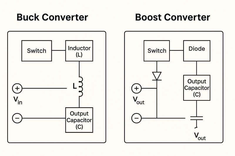
Both Buck and Boost Converters operate on the principle of inductive energy transfer. The main components include:
- Switch (MOSFET or Transistor): Rapidly turns ON and OFF to regulate voltage.
- Diode or Synchronous Switch: Maintains current flow when the main switch is OFF.
- Inductor (L): Stores and releases energy.
- Output Capacitor (C): Smooths voltage ripple and provides a stable DC output.
When the switch is ON, the inductor stores energy; when OFF, the same energy is supplied to the load or output capacitor. This working principle applies to both Buck and Boost converters.
1.2 Modes of Operation
Both converters primarily operate in two modes:
1️⃣ Continuous Conduction Mode (CCM): The inductor current never falls to zero. This mode provides low ripple and high stability.
2️⃣ Discontinuous Conduction Mode (DCM): The inductor current reaches zero at the end of each switching cycle. It is useful under light load conditions and reduces switching losses.
In power electronics design, CCM is usually preferred as it offers smoother output and simpler control.
2. Working Principle
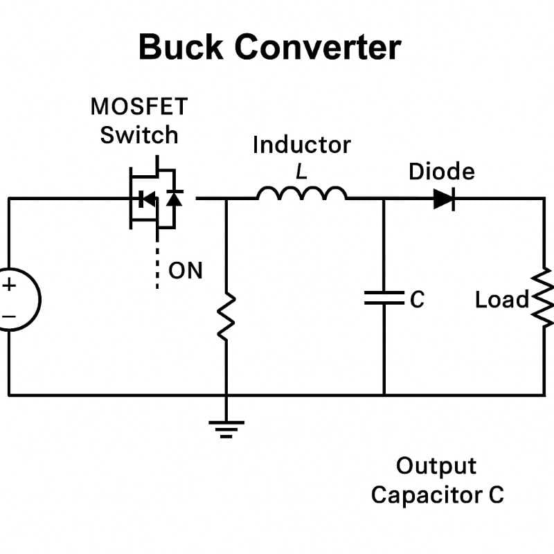
🔹 For Buck Converter:
When the MOSFET is ON, current flows through the inductor, and energy is stored in its magnetic field. When the MOSFET is OFF, the stored energy is delivered to the load through the diode (or synchronous MOSFET). As a result, the output voltage remains lower than the input.
Relation:
Vout = D × Vin
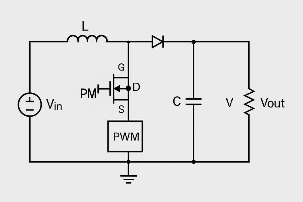
🔹 For Boost Converter:
When the MOSFET is ON, the inductor stores energy. When the MOSFET is OFF, the stored energy is released through the diode to the output capacitor and load, making the output voltage higher than the input.
Relation:
Vout = Vin / (1 – D)
2.1 Energy Flow
Both converters transfer energy through the magnetic field (inductive energy) rather than resistive dissipation. This is why their efficiency typically ranges between 85% and 95%.
Key Points:
- Buck Converter → Step-down voltage (Vout < Vin)
- Boost Converter → Step-up voltage (Vout > Vin)
Both converters work on the same principle — Energy Storage and Release through the Inductor.
3. Design Equations (Step-by-Step for Buck and Boost Converter Circuits)
In this section, we’ll understand how to calculate and select the main components (Inductor, Capacitor, MOSFET, etc.) for Buck and Boost Converter circuits using a step-by-step example. You can modify these steps based on your own input/output specifications.
3.1 Buck Converter Design Example
Given Specifications:
Input Voltage (Vin) = 12 V
Output Voltage (Vout) = 5 V
Output Current (Iout) = 2 A
Switching Frequency (fsw) = 100 kHz
Inductor Ripple Current (ΔIL) = 20% of Iout = 0.4 A
(a) Duty Cycle (D)
For a Buck Converter, the ideal relationship is:
Vout = D × Vin
D = 5 / 12 = 0.4167 (≈ 41.7%)
This means the switch remains ON for about 41.7% of each switching cycle.
(b) Inductor Value (L)
For Continuous Conduction Mode (CCM):
L = ((Vin – Vout) × D) / (fsw × ΔIL)
Substitute the values:
L = ((12 – 5) × 0.4167) / (100 × 10³ × 0.4) = 72.9 µH
🔹 Suggested Value: 75 µH (standard value)
(c) Output Capacitor (C)
C = ΔIL / (8 × fsw × ΔVout)
If ΔVout = 50 mV (0.05 V):
C = 0.4 / (8 × 100 × 10³ × 0.05) = 10 µF
🔹 Suggested Value: 22 µF or 47 µF capacitor for better ripple control.
(d) Diode or Synchronous Switch
- Non-synchronous converter: Use a Schottky diode.
- Synchronous converter: Use a low RDS(on) MOSFET in the freewheel path.
3.2 Boost Converter Design Example
Given Specifications:
Input Voltage (Vin) = 5 V
Output Voltage (Vout) = 12 V
Output Current (Iout) = 1 A
Switching Frequency (fsw) = 100 kHz
Inductor Ripple Current (ΔIL) = 25% of Iout = 0.25 A
(a) Duty Cycle (D)
For a Boost Converter:
D = 1 – (Vin / Vout)
D = 1 – (5 / 12) = 0.583 (≈ 58.3%)
This means the MOSFET remains ON for about 58.3% of each switching cycle.
(b) Inductor Value (L)
L = (Vin × D) / (ΔIL × fsw)
L = (5 × 0.583) / (0.25 × 100 × 10³) = 116 µH
🔹 Suggested Value: 100 µH – 120 µH inductor (ferrite core, low DCR).
(c) Output Capacitor (C)
C = (Iout × D) / (ΔVout × fsw)
If ΔVout = 50 mV (0.05 V):
C = (1 × 0.583) / (0.05 × 100 × 10³) = 116 µF
🔹 Suggested Value: 68 µF low ESR capacitor.
(d) MOSFET and Diode Selection
- MOSFET: Low RDS(on), 30–40V rated (IRLZ34N or IRFZ44N).
- Diode: MBR360 or SS36 (fast recovery, Schottky).
3.3 Design Summary
| Converter Type | L (µH) | C (µF) | Duty Cycle (D) | Efficiency Range (%) |
|---|---|---|---|---|
| Buck Converter | 75 | 22–47 | 0.4167 | 85–95 |
| Boost Converter | 100–120 | 68 | 0.583 | 80–90 |
4. Component Selection & BOM Recommendations for Buck and Boost Converter Circuits
The following Bill of Materials (BOM) tables are reference guides for selecting components for both Buck and Boost DC-DC Converter designs. These component choices will help you select the correct parts based on your voltage and current requirements.
⚙️ 4.1 Recommended Components for Buck Converter
| Component | Suggested Part | Remarks / Notes |
|---|---|---|
| High-Side MOSFET | IRLZ44N / IRLB3034 | Efficient MOSFET with low RDS(on) and high current rating. |
| Synchronous MOSFET (Optional) | Si7445 / Si7445DP | Low RDS(on) MOSFET to reduce conduction losses. |
| Diode (Non-Synchronous Case) | SS34 (Schottky Diode) | Low forward voltage drop; suitable for high-speed switching. |
| Inductor (L) | 75 µH, 5 A rated | Shielded power inductor for improved EMI performance. |
| Output Capacitor (Co) | 22 µF, 50 V (Low ESR) | Combination of ceramic (MLCC) and electrolytic reduces ripple. |
| Input Capacitor (Ci) | 100 µF, 25 V (Low ESR) | Provides input voltage stabilization and reduces switching noise. |
| Controller IC | LM2596 or equivalent | Required if using an external MOSFET (non-integrated switch). |
| Feedback Resistors | 10 kΩ + 3.3 kΩ | Divider network to set output voltage. |
⚙️ 4.2 Recommended Components for Boost Converter
| Component | Suggested Part | Remarks / Notes |
| Switching MOSFET | IRFZ44N / IRLZ34N | 60V rated, high-efficiency, low RDS(on) MOSFET. |
| Diode (Freewheeling) | MBR360 / SS36 | Fast recovery Schottky diode with low forward voltage. |
| Inductor (L) | 68 µH, 3 A rated | Low DCR ferrite-core inductor suitable for boost topology. |
| Output Capacitor (Co) | 47 µF, 25 V (Low ESR) | Reduces output ripple. |
| Input Capacitor (Ci) | 100 µF, 16 V | Maintains input voltage stability. |
| Controller IC | LM3478 / UC3843 | Popular PWM controller ICs for boost converter design. |
| Feedback Network | 33 kΩ + 10 kΩ | Resistor divider network to set desired output voltage. |
💡 Additional Recommendations
- Always choose Low ESR capacitors to minimize ripple and heating.
- When selecting MOSFETs, balance RDS(on) and Gate Charge (Qg) for optimal switching efficiency.
- Ensure the inductor’s saturation current exceeds the peak output current to prevent nonlinear behavior.
- Keep current loops short and maintain a solid ground plane in PCB layout to minimize EMI.
- In Boost Converters, pay extra attention to the thermal ratings of the inductor and diode.
🌍 Sourcing and Cost
These components generally fall into the low to medium cost range in both India and the USA. You can source them from the following reliable online suppliers:
- Mouser Electronics
- Digi-Key
- Element14 / Farnell
- LCSC Electronics
Each of these platforms provides datasheets, alternative models, and real-time pricing for the listed components.
5. Waveform Analysis of Buck and Boost Converter Circuits
To understand the operation of Buck and Boost Converter Circuits, analyzing their waveforms is essential. This analysis shows how voltage and current change during switching cycles and how these changes impact the converter’s stability, efficiency, and performance.
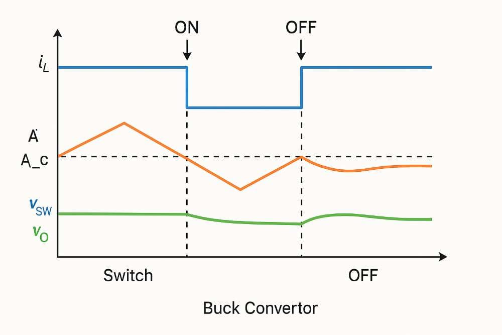
5.1 Analysis of Buck Converter ON–OFF Cycle
🟢 When the Switch is ON:
- Input voltage (Vin) is directly applied to the inductor (L) and the load.
- Inductor current increases linearly because the voltage across it is (Vin – Vout).
- The inductor stores energy in its magnetic field.
- The output capacitor (C) charges and smooths voltage ripple.
🔴 When the Switch is OFF:
- The MOSFET turns off, and current flows through the diode or synchronous MOSFET.
- The energy stored in the inductor is supplied to the load.
- The inductor current gradually decreases.
5.2 Analysis of Boost Converter ON–OFF Cycle
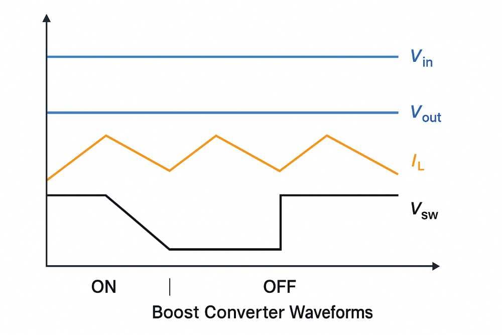
🟢 When the Switch is ON:
- Input voltage (Vin) flows through the inductor, storing energy in its magnetic field.
- The diode is reverse-biased, so the output capacitor continues to supply the load using its stored energy.
🔴 When the Switch is OFF:
- The inductor releases its stored energy through the diode to the output capacitor and load.
- During this phase, the output voltage becomes greater than the input voltage.
5.3 Key Waveforms in Buck and Boost Converters
1️⃣ Inductor Current (iₗ):
- The inductor current waveform is triangular in both converters.
- In a Buck Converter, current flows from input to output.
- In a Boost Converter, current is first stored in the inductor and then released to the output.
2️⃣ Inductor Voltage (vₗ):
- Buck Converter: Positive during ON, negative during OFF.
- Boost Converter: Negative during ON, positive during OFF.
3️⃣ Output Voltage (vₒ):
- Buck Converter → Nearly constant DC voltage (lower than Vin).
- Boost Converter → Output voltage higher than Vin.
4️⃣ Diode / Synchronous Switch Current:
- In a Buck Converter, current flows through the diode only during the OFF period.
- In a Boost Converter, diode current varies in both ON and OFF cycles and transfers charge to the output capacitor.
5.4 Difference Between CCM and DCM Waveforms
| Feature | CCM (Continuous Conduction Mode) | DCM (Discontinuous Conduction Mode) |
|---|---|---|
| Inductor Current | Never becomes zero | Becomes zero for part of the cycle |
| Ripple Current | Low | High |
| Efficiency | Higher under heavy load | Better under light load |
| Control Complexity | Simple | More complex |
Conclusion:
Most practical Buck and Boost Converters are designed to operate in CCM mode to reduce output ripple, maintain stable voltage, and simplify control.
5.5 Waveform Summary
- Inductor Current: Triangular waveform (increases and decreases linearly).
- Inductor Voltage: Square waveform (positive and negative swings).
- Output Voltage: Nearly constant DC waveform (lower for Buck, higher for Boost).
- Diode Current: Pulsed waveform (mainly active during OFF period).
By studying these waveforms, designers can ensure that the converter is stable, efficient, and delivers desired performance.
6. Efficiency Optimization Techniques for Buck and Boost Converter Circuits
The key advantage of Buck and Boost Converters is their high efficiency. These converters waste significantly less energy compared to linear regulators and can achieve 85%–95% efficiency. However, in practical circuits, several unavoidable losses occur, which must be understood and controlled.
6.1 Main Sources of Losses in Buck and Boost Converters
1️⃣ Conduction Losses:
Current flow through the MOSFET and diode causes resistive heating.
MOSFET Loss:
Pcond = I² × RDS(on)
Diode Loss:
Pdiode = I × VF
2️⃣ Switching Losses:
During each switching transition (ON/OFF), both voltage and current exist simultaneously across the MOSFET, leading to energy loss.
Switching losses are slightly higher in Boost Converters because current is greater on the input side.
3️⃣ Inductor Core and Copper Losses:
Core losses arise from magnetic hysteresis and eddy currents, while copper losses occur due to resistive heating of the inductor windings.
4️⃣ Gate Drive and Control Losses:
At high switching frequencies, gate charge/discharge in the MOSFET increases power consumption.
5️⃣ Capacitor ESR Losses:
The Equivalent Series Resistance (ESR) of the output capacitor causes ripple current heating.
6.2 Ways to Improve Efficiency
⚙️ 1. Use Low RDS(on) MOSFETs
A low RDS(on) MOSFET significantly reduces conduction losses.
Ensure the MOSFET’s voltage rating is 1.5–2× higher than the input voltage to avoid breakdown.
⚙️ 2. Use Schottky Diode or Synchronous Rectification
A Schottky diode has a low forward voltage drop (~0.3V), reducing conduction loss.
In synchronous converters (both Buck and Boost), replacing the diode with a MOSFET can improve efficiency by 5–10%.
⚙️ 3. Choose an Optimal Switching Frequency
- Very high frequency → increases switching losses.
- Very low frequency → requires larger inductors and capacitors.
Ideal range: 50 kHz – 200 kHz (depending on the application).
⚙️ 4. Use High-Quality Inductors and Capacitors
- Low ESR capacitors reduce output ripple and heating.
- Ferrite core inductors minimize hysteresis and eddy current losses.
- In Boost converters, ensure the inductor has adequate saturation current capacity.
⚙️ 5. Optimize PCB Layout
- Keep the power loop (MOSFET–Diode–Inductor–Capacitor) short and wide.
- Place input/output capacitors close to the MOSFET.
- Maintain a solid ground plane to reduce EMI and resistive losses.
⚙️ 6. Thermal Management
- Use heat sinks or copper pours under the MOSFET and diode.
- For high-power circuits, add forced-air cooling (fan).
- In Boost converters, monitor MOSFET heating carefully as it is typically higher.
6.3 Typical Efficiency Range
| Load Condition | Buck Converter Efficiency | Boost Converter Efficiency |
|---|---|---|
| Light Load (20%) | 75–85% | 70–80% |
| Medium Load (50%) | 85–92% | 80–88% |
| Full Load (100%) | 90–95% | 85–90% |
7. Practical Design Tips & Testing Methods for Buck and Boost Converter Circuits
Understanding the theoretical design of Buck and Boost Converters is important, but their practical implementation is equally critical. When building the real circuit, certain additional precautions and testing procedures must be followed to ensure the converter remains stable, efficient, and reliable.
🧩 7.1 Practical Design Tips
⚙️ 1. Pay Attention to PCB Layout
- Keep the Power Loop Short: Minimize the trace length between the input capacitor, MOSFET, diode, and inductor to reduce EMI and switching noise.
- Use a Strong Ground Plane: Connect all high-current paths to a common ground plane to reduce voltage drop and noise.
- Separate Signal and Power Grounds: Create a separate signal ground for the feedback circuitry and connect it to the power ground at a single star point.
⚙️ 2. Shield the Feedback Network
- Place feedback resistors away from noisy nodes (such as the switching node or inductor).
- Keep the feedback trace short and shielded to ensure accurate voltage sensing.
- Use an RC compensation network for stable voltage feedback in both Buck and Boost converters.
⚙️ 3. Improve Output Filtering
- Use a combination of Low ESR and high-frequency ceramic capacitors.
- Add an LC or π-filter for high-ripple applications.
- In Boost converters, pay special attention to the capacitor ripple current rating.
⚙️ 4. Thermal Management
- Place thermal vias or copper pours under the MOSFET and diode to improve heat dissipation.
- If the converter handles 2A or more current, use heat sinks or forced-air cooling.
- In Boost converters, the MOSFET and diode temperatures are typically higher—ensure proper cooling.
⚙️ 5. EMI Reduction Techniques
- Keep the switching node (SW) compact and avoid placing a ground plane directly underneath.
- Add an RC snubber circuit to reduce ringing and EMI.
- Use a π-filter or common-mode choke at the input to suppress input noise and harmonics.
⚙️ 7.2 Testing Methods
1️⃣ No-Load and Full-Load Testing
- Run the converter under no-load conditions and measure the output voltage.
- Gradually increase the load until reaching full-load conditions.
- If voltage regulation remains stable, the design is successful.
2️⃣ Ripple Measurement
- Measure the output ripple using an oscilloscope.
- Keep the ripple ≤ 50 mV (p-p).
- In Boost converters, ripple may be slightly higher due to higher output voltage.
3️⃣ Efficiency Measurement
- Formula:
Efficiency (%) = (Vout × Iout) / (Vin × Iin) × 100 - Typical efficiency:
Buck Converter: 85–95%
Boost Converter: 80–90%
4️⃣ Thermal Testing
- Use an infrared thermometer or thermal camera to measure component temperatures.
- Keep MOSFET and inductor temperatures below 100°C.
5️⃣ Transient Response Testing
- Apply a sudden load change (e.g., 0.5A → 2A) and observe the output voltage.
- A good design will show <5% transient deviation.
🧠 7.3 Common Troubleshooting Tips
| Problem | Possible Cause | Solution |
|---|---|---|
| Output voltage too low | Incorrect duty cycle or feedback resistors | Check the feedback divider network |
| High output ripple | Low inductor or capacitor value | Use higher-value or low ESR capacitors |
| Overheating | High MOSFET RDS(on) or poor airflow | Use low-loss MOSFETs and add heat sinks |
| Oscillation / Instability | Poor feedback layout or wrong compensation | Improve PCB layout and adjust compensation network |
| Boost output drop | Inductor saturation or diode heating | Use higher current-rated inductors and fast-recovery diodes |
8. PCB Layout & EMI Mitigation Tips
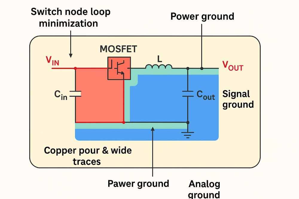
- Keep the switch loop small (MOSFET–Diode–Inductor loop).
- Grounding: Separate power and signal grounds; connect at a single star point.
- Place decoupling capacitors close to the MOSFET.
- Add an RC snubber network to reduce ringing.
- Use π-filters and common-mode chokes for EMI reduction.
- Ensure good thermal design with heat sinks, via stitching, and copper pours.
9. Conclusion
In this tutorial, we learned all the essential aspects of Buck and Boost Converter Circuits step-by-step:
- Buck Converter: Step-down voltage regulation.
- Boost Converter: Step-up voltage regulation.
- Design, working principle, waveform analysis, simulation, and PCB layout.
Key Takeaways:
For Buck Converter:
Vout = D × Vin
For Boost Converter:
Vout = Vin / (1 – D)
To achieve higher efficiency, use low-loss components and ensure optimized PCB layout.
Verify theoretical and practical performance through LTSpice or Simulink simulation.
FAQ
What is the working principle of a Buck and Boost Converter?
The Buck and Boost Converter works by controlling the energy stored in an inductor. During the ON period of the switch, the inductor stores energy, and during the OFF period, it releases this energy to the load. By adjusting the duty cycle, the converter steps up or steps down the voltage.
What are the applications of a Buck and Boost Converter?
Buck and Boost Converters are widely used in power electronics circuits such as DC power supplies, battery charging systems, solar energy systems, LED drivers, and electric vehicles.
What are the advantages of a Buck and Boost Converter?
It offers high efficiency, compact design, wide input voltage range, and stable output under varying load conditions — making it ideal for portable and renewable energy systems.
What is the difference between Buck and Boost Converter?
A Buck Converter steps down the voltage (Vout < Vin), while a Boost Converter steps up the voltage (Vout > Vin). A Buck-Boost Converter can perform both functions depending on the duty cycle.
